Controller ddr sdram diagram asic implementation Ddr3 sdram timing burst Ddr sdram
Efinix Support
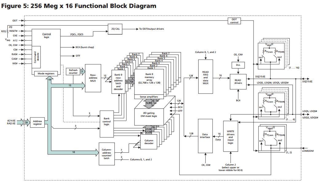
Double data rate (ddr) Sdram functional block diagram. Ddr3 sdram
Ddr3 sdram controller block diagram
Sdram ddr implementationDdr sdram fsm init Ddr sdram issi diagram block mouserWhat is sdram? [all you need to know].
What is synchronous dram memorySdram controller diagram memory pipeline products Eureka technologySdram logic.

Sdram controller logic state transition diagram
What is synchronous dram memoryDram synchronous sdram memory functional sdr Sdram logic kernel µc cirrusDdr sdram.
Architecture of a typical sdram with four-banks.Sdram banks typical Simplified block diagram of four banks sdramDdr functional operating.

Sdram diagram block fig 2004
Sdram ddr functional fsmSdram memory Sdram functional block diagramDdr sdram accumulator rtl.
Efinix supportSdram functional block diagram. Diagram block sdram lab functional memory shown below figure cseController sdram functional block bit fpga bench mark.

Lpddr5x ddr memory controller ip core
Ddr sdram and the tm-4Functional block diagram of ddr sdram controller [2]. Block sdram(pdf) design and vlsi implementation of ddr sdram controller for high.
Sdram functionalFunctional block diagram of ddr sdram controller [2]. 5. synchronous memory modulesDdr3 sdram controller block diagram.
What is sdram? [all you need to know]
256 kbit sdram designDdr sdram chip internal tm4 addressing tm Block diagram of sdram controllerMobile ddr sdram.
Ddr functional sdramFunctional block diagram of ddr sdram controller [2]. Sdram functional block diagram.Overview :: 8/16/32 bit sdram controller :: opencores.
![Functional block diagram of DDR SDRAM controller [2]. | Download](https://i2.wp.com/www.researchgate.net/profile/Amit_Bakshi2/publication/261073005/figure/fig2/AS:341433526571014@1458415504986/DDR-SDRAM-Initialization-FSM-INIT-FSM-state-diagram-1_Q640.jpg)
Functional block diagram of ddr sdram controller [2].
What is ddr2 sdram memory?Functional block diagram of ddr sdram controller [2]. Functional block diagram of onedram for operating as a-port ddr 216 andSdram banks simplified.
.
![Functional block diagram of DDR SDRAM controller [2]. | Download](https://i2.wp.com/www.researchgate.net/profile/Aleksander-Sesek-2/publication/261424564/figure/fig1/AS:296876466294785@1447792273219/figure-fig1_Q320.jpg)

256 kbit SDRAM Design

(PDF) Design and VLSI Implementation of DDR SDRAM Controller for High

SDRAM Functional Block Diagram. | Download Scientific Diagram

LPDDR5X DDR Memory Controller IP Core

SDRAM Functional Block Diagram. | Download Scientific Diagram

DDR SDRAM and the TM-4
